
Which of the following diagrams doesn't show AND gate?
Answer & explanation
Correct answer: option 2
The correct answer is Option (2)
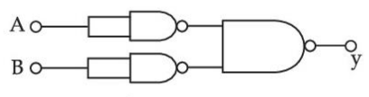
Find the output y of each circuit in terms of A and B, using De Morgan’s theorem, \( \overline{P+Q} = \bar{P}\cdot\bar{Q} \) and \( \overline{P\cdot Q} = \bar{P}+\bar{Q} \). A NAND or NOR gate with its two inputs joined acts as a NOT gate.
Option (2) — each input goes to a NAND gate with its inputs joined, which is a NOT gate, and the two results go to a NAND gate:
\( y = \overline{\bar{A}\cdot\bar{B}} = A + B \)
This is an OR gate, not an AND gate.
Why the other options are incorrect
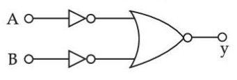
Option (1) — Incorrect. Both inputs are inverted and then fed to a NOR gate: \( y = \overline{\bar{A}+\bar{B}} = A\cdot B \). This is an AND gate, so it is not the answer.
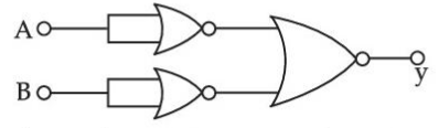
Option (3) — Incorrect. Each input goes to a NOR gate with its inputs joined (a NOT gate), then to a NOR gate: \( y = \overline{\bar{A}+\bar{B}} = A\cdot B \). This is an AND gate.

Option (4) — Incorrect. A NAND gate is followed by a NAND gate with its inputs joined (a NOT gate): \( y = \overline{\overline{A\cdot B}} = A\cdot B \). This is an AND gate.