When a forward bias is applied to a p-n junction diode, then,
(A) majority carrier current becomes zero.
(B) potential barrier is raised.
(C) width of the depletion layer reduces.
(D) junction resistance increases.
Choose the correct answer from the options given below:
Answer & explanation
Correct answer: option 2
The correct answer is Option (2) → (C) only
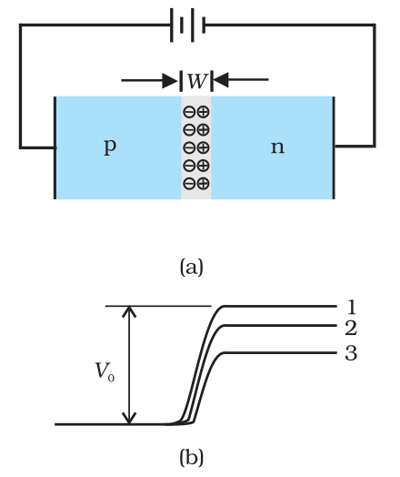
In forward bias the p-side is connected to the positive terminal. The applied voltage V opposes the built-in barrier potential, so the effective barrier falls to \( V_0 - V \). Majority carriers can then cross the junction easily, the depletion layer narrows, and a large current flows.
(A) majority carrier current becomes zero. — Incorrect. The majority carrier current becomes large; it is the forward current of the diode.
(B) potential barrier is raised. — Incorrect. The barrier is lowered, to \( V_0 - V \); it is raised in reverse bias.
(C) width of the depletion layer reduces. — Correct. Carriers pushed towards the junction neutralise part of the uncovered ions, so the depletion layer becomes narrower.
(D) junction resistance increases. — Incorrect. With a lower barrier and a large current, the junction resistance decreases.
NCERT (2026-27):
p-n Junction Diode Under Forward Bias – “When an external voltage \( V \) is applied across a semiconductor diode such that p-side is connected to the positive terminal of the battery and n-side to the negative terminal [Fig. 14.13(a)], it is said to be forward biased. … The direction of the applied voltage (\( V \)) is opposite to the built-in potential \( V_0 \). As a result, the depletion layer width decreases and the barrier height is reduced [Fig. 14.13(b)].”