
CUETMOCK
  • Pricing
  • Mentors
Log inStart freeStart free mocks→

First test, then trust

Try a free CUET mock test.

Join 5,00,000+ students who rehearsed exam day on the exact NTA screen before sitting CUET. On the web and on Android.

Start free mocks →Get the Android app
CUETMOCK

India's #1 CUET Mock Test Platform. Original NCERT-based questions on the exact NTA exam screen — trusted by 5,00,000+ students since CUET 2022.

Get it onGoogle PlayScan to download the CUETMOCK app

Mock tests

  • CUET mock test series
  • Commerce mocks
  • Humanities (Arts) mocks
  • Science mocks
  • Languages & GAT mocks
  • Free practice questions
  • Pricing

Resources

  • CUET exam guide
  • CUET syllabus
  • Universities accepting CUET
  • Expert blogs
  • News & notifications
  • Webinars & counselling
  • CUET score calculator
  • How we estimate your rank
  • FAQs

Company

  • About us
  • Our leadership & team
  • Our toppers
  • Mentors
  • For schools
  • Contact us
  • Terms
  • Privacy
  • Refund policy

Talk to us

+91 7696 6630 56info@cuetmock.comWhatsApp us

Our other platforms

  • JEE Mock — For IIT-JEE aspirants
  • NEET Mock — For NEET aspirants

Newsletter

Exam updates, study material and offers — no spam.

© 2026 NYC Ventures Pvt. Ltd.

701-702, Royal Business Park, Zirakpur, Punjab - 140603

  • Terms of use
  • Privacy policy
  • Refund policy
  • Contact us

iCUETMOCK is an independent preparation platform, not affiliated with the National Testing Agency (NTA). Always check exam details on the official NTA website.

  • Home
  • Mock tests
  • CUET guide
  • Pricing
  • Log in
Home/Practice questions/Physics
PhysicsSemiconductors and Electronic Devices

Which of the following statements about the depletion region of an un…

Which of the following statements about the depletion region of an unbiased p-n junction are correct?

A. The width of the depletion region is independent of the densities of the dopants.
B. The width of the depletion region is dependent on the densities of the dopants.
C. The electric field in depletion region is produced by the positive and negative ions.
D. The electric field in the depletion region is produced by the electrons in the conduction band and the holes in the valence band.

Choose the correct answer from the options given below:

Answer & explanation+

Correct answer: option 4

The correct answer is Option (4) → B and C only

When a p-n junction forms, electrons and holes diffuse across and recombine near the junction. This leaves a thin depletion region containing only immobile ions: positive donor ions on the n-side and negative acceptor ions on the p-side.

(A) The width of the depletion region is independent of the densities of the dopants. — Incorrect. With heavier doping the required ion charge is found in a thinner layer, so the region becomes narrower.

(B) The width of the depletion region is dependent on the densities of the dopants. — Correct. This is the reason given for (A).

(C) The electric field in depletion region is produced by the positive and negative ions. — Correct. The uncovered donor and acceptor ions set up the field (the barrier) across the junction.

(D) The electric field in the depletion region is produced by the electrons in the conduction band and the holes in the valence band. — Incorrect. The region is depleted of mobile charge carriers; free electrons and holes are not what produce its field.

NCERT (2026-27):
p-n Junction Formation – “… When an electron diffuses from n → p, it leaves behind an ionised donor on n-side. This ionised donor (positive charge) is immobile as it is bonded to the surrounding atoms. … Similarly, when a hole diffuses from p → n due to the concentration gradient, it leaves behind an ionised acceptor (negative charge) which is immobile. … This space-charge region on either side of the junction together is known as depletion region as the electrons and holes taking part in the initial movement across the junction depleted the region of its free charges …. … Due to the positive space-charge region on n-side of the junction and negative space charge region on p-side of the junction, an electric field directed from positive charge towards negative charge develops.”
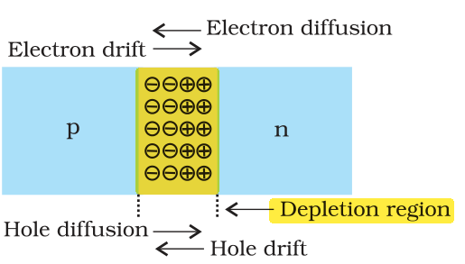
Textbook figure

Advertisement

Practise more on Semiconductors and Electronic Devices

Chapter-wise mocks on the real NTA exam screen, with solutions and your rank. Your first mocks are free.

Start free mocks →

Advertisement

Next questions

  1. Arrange the correct sequence of the following steps involved in the Selection process.(A) Employment Interview(B) Aptitude Test(C) Referenc…Business Studies · Staffing
  2. The organising function leads to the creation of an organisation structure. Which of the following does this structure include?(A) Designin…Business Studies · Organising
  3. In a class of 40 students, Anjali's rank is thrice that of Anita. There are 4 students who have ranks worse than that of Anjali. Anita's ra…General Aptitude Test · Verbal Reasoning
  4. In which of the following years was ADB (Asian Development Bank) established?General Aptitude Test · General Knowledge
  5. Identify the correct order of showing following current assets in Balance sheet of a company: (A) Other current assets(B) Inventories(C) Cu…Accountancy Part B · Financial Statements of a Company
  6. Select the market in which shares are traded :Business Studies · Financial Markets
  7. How will you treat payment of dividend in a Cash flow statement?Accountancy Part B · Cash Flow Statement
  8. Which of the following reaction can be used to convert acetamide to methyl amine?Chemistry · Organic: Amines
  9. Which of the following combinations of measures of quantity and unit is NOT a correct match?General Aptitude Test · General Knowledge
  10. Read the following statements. I. The generative cell is larger and contains a significant amount of food reserves. II. The vegetative cell…Biology · Sexual Reproduction in Flowering Plants