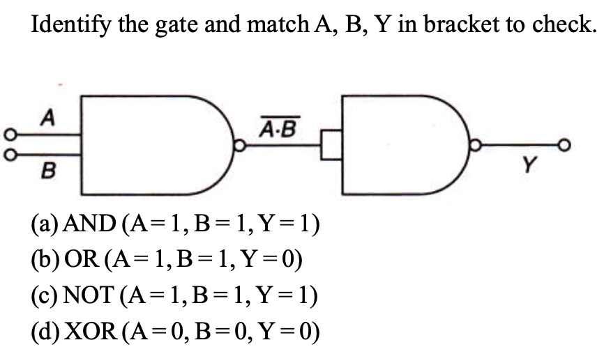
The given diagrams involve 2 gates.
The first 1 is an AND gate followed by a NOT Gate, with the compliment of the output of first gate used as an input to the other gate which is NAND gate as NOT gate.
We consider the 4 combinations
A=1,B=1,AB=1,(AB)′=0,$\bar{AB} = 1$,Y=0
A=1,B=0,AB=0,(AB)′=1,$\bar{AB} = 0$,Y=1
A=1,B=0,AB=0,(AB)′=1,$\bar{AB} = 0$,Y=1
A=0,B=0,AB=0,(AB)′=1,$\bar{AB} = 0$,Y=1
The above configuration represents that of an AND gate. |