
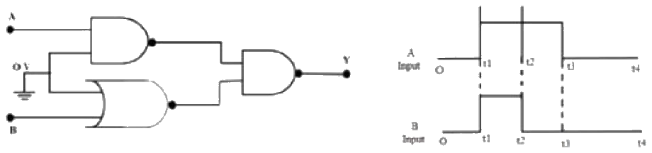
Sketch the output Y for the circuit shown below for two inputs.
Answer & explanation
Correct answer: option 3
The correct answer is Option (3)
Work out the Boolean output of each gate, with the 0 V line as a fixed input 0. The two input gates are a NAND gate (AND symbol with a bubble) and a NOR gate (OR symbol with a bubble), and the output gate is a NAND gate.
Upper gate, NAND of A and 0: an AND with a 0 input is always 0, so its NAND is always 1.
\( \displaystyle Y_{1} = \overline{A \cdot 0} = \overline{0} = 1 \)
Lower gate, NOR of 0 and B:
\( \displaystyle Y_{2} = \overline{0 + B} = \overline{B} \)
Output gate, NAND of \( Y_1 \) and \( Y_2 \):
\( \displaystyle Y = \overline{1 \cdot \overline{B}} = \overline{\overline{B}} = B \)
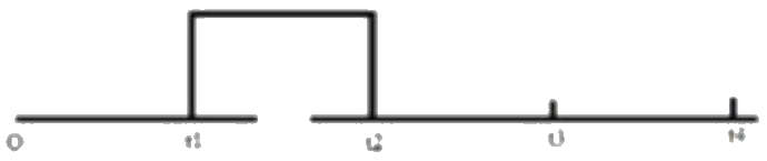
So the output simply follows input B. From the waveforms, B is high only between \( t_1 \) and \( t_2 \), so Y is a single pulse from \( t_1 \) to \( t_2 \) and is low elsewhere. Option (3) shows exactly this pulse.